
The following article was written by Barbara Foster, president of "Microscopy, Marketing & Education", Springfield, MA. and Barry Fookes, president, "Gordon-Grau Scientific Inc.", Kissimmee, FL. It originally appeared in the February, '96 issue of ASM International's Advanced Materials & Processes magazine. It is reproduced here with the kind permission of Margaret Hunt, editor of Advanced Materials & Processes.
The combination of new technologies, new software approaches, and expansion
of analytical techniques to include more automated stereology is expanding
the ability of materials scientists to define microstructure and determine
its effect on function.
Recent advances in both computer and camera electronics combined with older
but less accessible stereological analyses are opening new venues for
microstrucural analysis. The most important areas of impact for these advances
are a better understanding of the structure/function relationship and resulting
process control. This article reviews some of the current trends in technology
and cites several applications of stereology.
Windows-based technologies
For decades, microstructure has been analyzed quantitatively through either
laborious manual methods or fully integrated image analysis systems. However,
advances in desktop computers and Windows-based software are opening new
opportunities for customized systems. These are built from components and
configured by system integrators or value-added resalers who carry a range
of cameras and monitors, digitizing boards, and software solutions. The new
systems can be built onto or networked with existing computers, saving money
and minimizing training.
These advances also enable software developers to offer greater functionality
at lower cost. The Windows interface provides a venue for control of peripherals
such as scanning stages (x, y positioning and scanning patterns) and focus
(z), shutters, and filterwheets, considerably reducing the time necessary
for generating computer code. Microscope companies such as Nikon and Zeiss
have been taking advantage of this Windows feature for the past several years.
Recently, off-the-shelf software companies such as
Optimas and
Media Cybernetics (Image Pro Plus, Fig.
1) have built new control modules into their packages, specifically for the
stages and other peripherals offered through Prior Scientific and Ludl Electronic
Products.
| Fig. 1 (right) - Image Pro Plus has built new control modules into their packages, specifically for the stages. | |
Windows-based programming also expands report-writing capabilities, readily
integrating text, images, graphics, and data as well as extending control
from desktop computers to the process line. Analysis, reporting, and process
control from one central location or via a network is now a reality.
New camera technologies
Development of this new generation of custom integrated systems has also
been spurred by advances in camera technology, Cameras such as the Leaf Lumina,
and combined camera/electronic systems such as those available from Dage-MTI,
offer greater resolution at lower prices. In addition, advances in color
technology enable use of software packages offering true color segmentation
in addition to traditional thresholding by gray-level.
The next challenge for designers will be to provide increased computer processing
capability to match the larger image formats from these cameras. Current
minimum standards for "high resolution " image are 512 x 512 pixels in
black-and-white mode, requiring that the computer system handle a quarter
of a megabyte of data per image. However, higher XY resolution capability
is pushing that requirement rapidly into the one to four megabyte range.
Adding color multiplies that requirement by nearly an order of magnitude,
stressing all but the workstation and mainframe platforms. Materials scientists
new to image analysis or considering expansion of existing systems should
carefully assess their needs and the ability of the computer portion of their
system to handle the output and processing requirements of these new
technologies.
Innovative approaches
Windows technology is not the only advance on the programming front. The
new direction in "shrink-wrapped" software is toward application-specific
packages. In the most progressive systems, such as those offered through
Media Cybernetics recently released Mat Pro Materials Science Module, the
interface uses conventional materials science terminology and follows standard
protocols. This approach simplifies analysis by isolating key steps.
Both the more expensive fully integrated systems and the off-the-shelf software
provide the ability to construct macros, lists of instructions that automate
routine tasks, In most cases, no programming or even typing skills are required.
Rather, a mouse is pointed at the appropriate function and simply clicked
to add that step to the instruction list.
Although some systems still rely on gray-level thresholding, many manufacturers
are expanding their programs to include real color, an advantage in many
semiconductor applications, polarized light analyses, and certain acid-etched
metallic surface studies. Other systems, such as Context Vision, are even
segmenting based on texture.
Grain-boundary completion has always been a challenge for more automated
systems, but advanced software such as Visilog (Noesis) and software/hardware
solutions such as Imagist (Princeton Gamma Tech) solve the problem. For example,
Noesis uses a novel combination of watershed and reconstruction algorithms
to reconstruct the missing grain boundary, while PGT has incorporated a version
of artificial intelligence to make local comparisons between hypothetical
images to reconstruct the missing grain boundary.
Changing microscopy
In a radical departure from conventional microscope design, prototypes now
available through General Scanning Inc. (GSI) and materials sciences instruments
from Biomedical Photometrics Inc. are built specifically for examining
ultra-large fields of view and for high-throughput situations.
As shown below, the field of view (FOV) for a conventional microscope may
be calculated by dividing the field number engraved on the eyepiece (usually
ranging from 18 mm to about 26 mm in newer metallographs) by the total
magnification of the objective and any intermediate optics.
FOV = field number /( Mobj * Mint)
For example, for a IOX objective viewed with an eyepiece having a field number
26, the field of view is 2.6 mm. While an objective of this type will have
a reasonable working distance (2.3 to about 7 mm), its resolution would be
limited to somewhere between 0.75 and 1.4 um.
In comparison, specifications on the new large-format microscopes are impressive.
By clever application of electronics, they require only one objective to
scan magnifications from 1X (5 x 5 gm) to 10OX (500 x 500 mm or IX FOV) on
a 1024 x 1024 display. An electronic pan mode enables the viewer to see any
portion of the field on demand. Spectrally, they detect color from the near
ultra-violet through the visible spectrum (365 to 680 nm). The GSI system,
for example, provides a numerical aperture of 1.00 (the theoretical limit
for non-immersed optics), offering submicron resolution (Rxy = 0.5 um) over
a 5 mm field of view, with a 3 to 4 mm working distance, a remarkable combination
of specifications.
For those applications in which information is obscured by glare or haze
(rough surfaces or polyurethane foams), both microscopes can operate in confocal
mode, cleanly imaging these previously inaccessible structures.
Structure-function relationships
The greatest impact of the new technologies is on a stronger understanding
of the structure-function relationship in materials, and on the ability to
translate data gathered from microstructures into better process control.
Traditionally, much image analysis has been based on the geometric information
(area, perimeter, projection, etc.) derived from the feature-specific analyses
in morphometry. While the histograms of population distributions generated
by this approach can be valuable, all too often they fall short of truly
describing the bulk properties that influence mechanical strength, thermal
sensitivity, and other properties.
Stereology provides the necessary field-oriented analyses, but it requires
of a large number of fields to be statistically valid. Currently, relatively
few automated image analysis systems include any stereology, necessitating
hours of tedious manual work. To further complicate matters, the mathematical
proofs behind this method are extremely challenging. Texts written on the
subject are aimed at communication within that field of mathematics rather
than for the lay user, making entry daunting, and masking relevance to everyday
applications.
Ironically, the actual measurements needed for stereology are extremely simple
and available in the digitized images common to all image analysis packages,
and the actual math is trivial and easily inserted. The result is a body
of parameters that provide strong relationships between structure and function.
They can be readily translated into process control of factors such as time
at temperature, moisture content, and concentration of constituent or catalyst.
| Fig. 2 (right) - A stereological application using Optimas software to determine grain size. In the example shown here, users may choose between cycloid, grid, or diagonal line patterns. |  |
Sizing operations
The ability to characterize powders, grain and cell sizes, and separated
features within a microstructure falls under the generic term "Sizing." Since
micro-features are often irregular in size, shape, and orientation, no single
parameter can be used to characterize their true form. However, for the
population distributions typical of morphometry, if the shapes of features
are known, then size distributions can be derived, and vice versa.
For regular polygonal grain structures, individual components can be assumed
to have a pseudo-spherical shape, and a simple intercept length and area
measurement on individual features, recorded from the plane section, can
be used to define the grain size distributions.
For example, to evaluate ferrite grain size in low-carbon steels, sizing
can be done by the linear intercept method. In this approach, a test pattern
of lines of known length is randomly laid over a plane section, and the
individual intercept lengths across features of interest are measured. The
data is ranked, then grouped into an arbitrarily determined number of size
bins (such as 10 bins) of set size increment (such as 2.5 um).
The image presented by the plane section will be that of grains having a
superimposed test line (pattern). The pattern intercepts the grains and produces
chords of varying lengths, with a maximum length equal to the diameter of
the sphere. Using the working relationship shown below, the number of intercepts
per unit test length (NL)can be used to find the number of grains of a specific
size per unit volume of the sample:
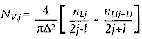
Where j=class, Nvj = number of grains/volume in that class size, nL= number of intercepts/test line in that class, and delta=2.5 x 10⁻³mm, the intercept size range.
| Group #, j | Intercept size range Delta, um |
Number, NLf/mm |
Grain dia. Dj, X10-3 mm |
No. of grains (X105) per mm3, Nvj |
Percentage |
|---|---|---|---|---|---|
| 1 | 0.0-2.5 | 6 | 2.5 | 68 | 5 |
| 2 | 2.5-5.0 | 17 | 5.0 | 177 | 15 |
| 3 | 5.0-7.5 | 24 | 7.5 | 426 | 35 |
| 4 | 7.5-10 | 19 | 10.0 | 259 | 21 |
| 5 | 10.0-12.5 | 13 | 12.5 | 146 | 12 |
| 6 | 12.5-15 | 8 | 15.0 | 70 | 6 |
| 7 | 15.0-17.5 | 5 | 17.5 | 24 | 2 |
| 8 | 17.5-20.0 | 4 | 20.0 | 19 | 1.5 |
| 9 | 20.0-22.5 | 3 | 22.5 | 14 | 1 |
| 10 | 22.5-25.0 | 2 | 25.0 | 21 | 1.5 |
For example, using the data from the table, terms for the fifth group give:
Nv5 = 2.04X10⁵ [13/(10 - 1) - 8/(10+1)] = 146xlO5 grains/mm3
These results are based on only 101 intercept measurements, yet they are statistically valid. In other words, accurate grain measurements may be achieved without expensive equipment, by the use of an optical microscope, a simple counting technique, and a ruler.
Go To: |
[Home] |
[ AM&P Articles] |
[Metallography FAQ] |